
We use cookies to provide great user experience. By continuing on this site you accept use of the cookies.
We use cookies to provide great user experience. By continuing on this site you accept use of the cookies.


The creation of different surface structures with sub-micron precision and a high-resolution direct-write laser and electron beam lithography method for various applications.
Materize offer electron beam lithography service based on ultra high resolution Raith eLINE Plus system. It gives us ability to manufacture structures with resolution down to 10 nm with quick turnaround time.
We offer pattern design and accept designs in various formats including GDS II, dxf etc. Traxx and periodixx features allows to pattern large stitch-free structures.
Direct-write laser lithography can be used to fabricate masks for mask-lithography and to draw optic waveguides or micro-lenses. It can be used in nanowire research, microfluidics, and metamaterials as well as to make stamps for holograms or any other application that requires high-precision, high-resolution microstructures.
Examples produced in our facilities include an organic optical modulator, fabrication of micro-lenses, and substrates for measurements of nanowire mechanical properties.
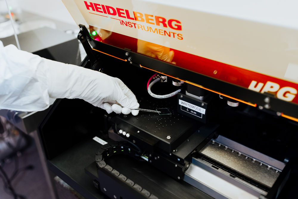
The central device in the optical lithography workflow is the micro pattern generator ‘µPG 101’ from ‘Heidelberg Instruments’. With working wavelength λ = 375 nm, substrates can be used up to 6″ x 6″, structures can be made down to 0.6 µm, recording resolution is 200 nm and max device height is 6mm. Resists used – positive AZ1518, AZ1050, SPR700 and negative SU-8: GM-1075, SU-8: SU8-2002.
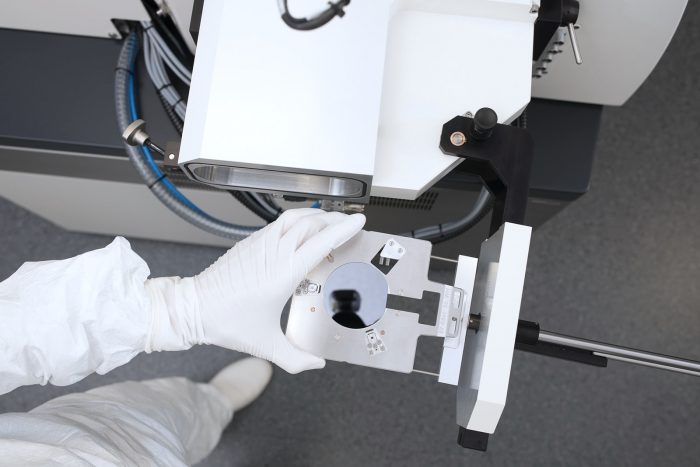
All micro lens device preparation processes take place in a laminar flow cabinet. This starts with cleaning the substrate. The substrate is then covered with a photoresist using a spin-coater placed in a laminar flow cabinet; it is then gradually heated to evaporate the solvent and subsequently placed in a ‘µPG 101’ system to illuminate cylindrical structures with a diameter of about 40 microns. The photoresist is exposed after two minutes to create the cylindrical structures. After exposition, the photoresist is heated to round off the cylindrical structures and create micro-lenses. After the fabrication process, micro-lenses are examined in Zygo NewView 7100 Optical Surface Profiler to verify the quality of the lenses.
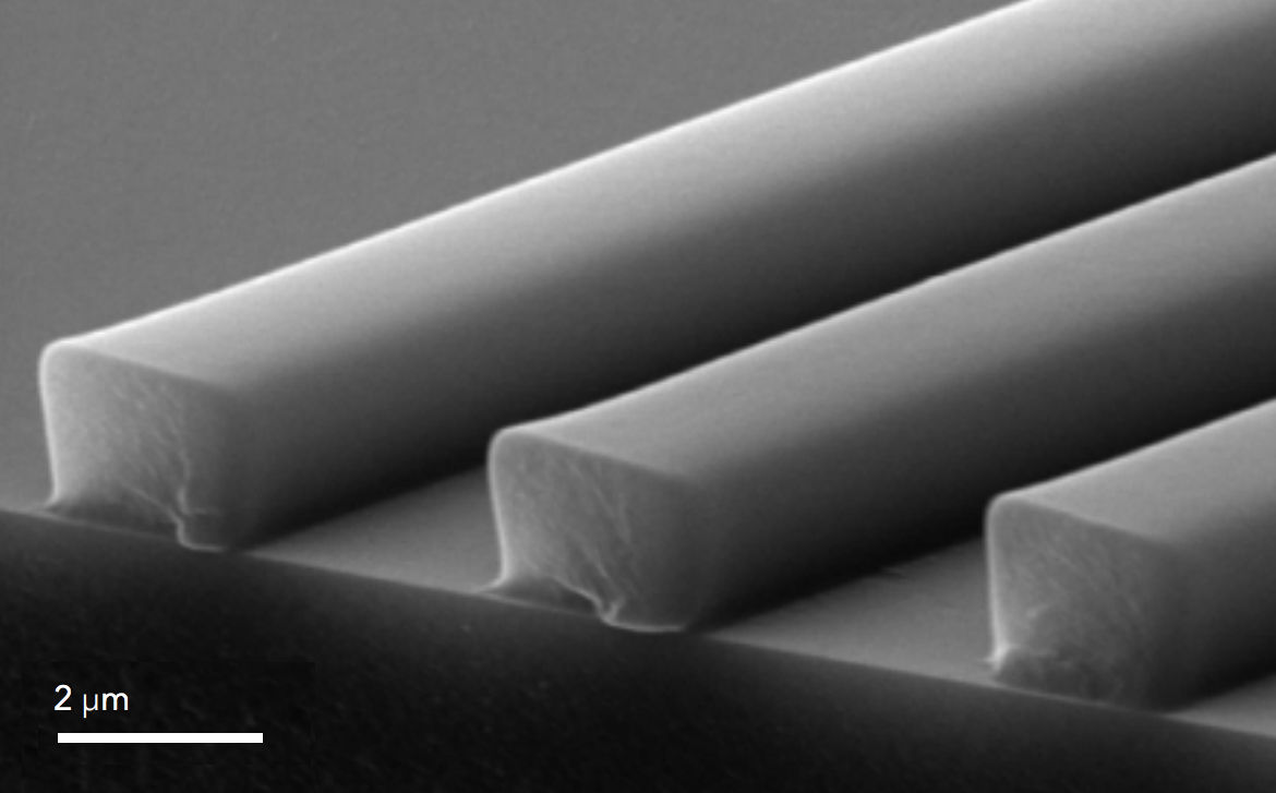
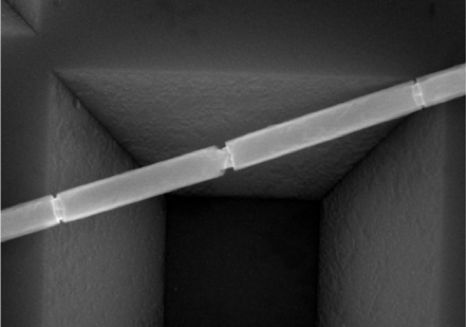
1-dimensional (1D) nanomaterials (nanowires, nanotubes, nanofibres) have a wide range of applications: from nano-electronics to textiles and composite materials. Mechanical properties (strength, durability, etc.) of 1D nanomaterials are important for multiple applications, such as metal nanowire-based flexible electronics. Nano-mechanical properties of 1D nanostructures can be determined, for example, using atomic force microscopy (AFM) by the 3-point bending tests carried out on these 1D nanostructures deposited on a specific substrate surface. Laser direct writing lithography equipment makes customised substrates for mechanical tests of nanowires using a semiconductor silicon wafer as the substrate material.
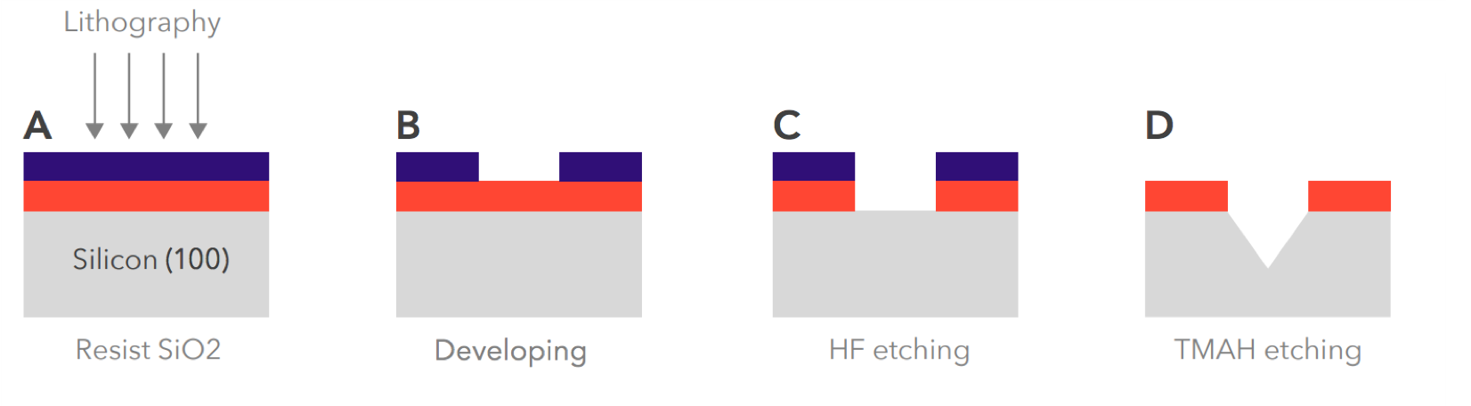
The simplified technological sequence consists of spin-coating the photoresist on a silicon wafer with a thermal oxide; writing (exposure) of the designed pattern using photolithography equipment; chemical development of the photoresist and its baking; etching of unprotected silicon oxide (silica mask formation); anisotropic etching of unprotected regions of the silicon surface; photoresist stripping; dissolution of the remaining silicon oxide and wafer rinsing; cutting of silicon wafer in pieces (each piece is a finished substrate).
We have established a workflow for the development and testing of active and passive optical waveguide devices. Waveguides are optical elements used for guiding light. We show an electro-optical (EO) modulator which was prepared using two optical lithography steps. The top and side views of the modulator design are as depicted below.
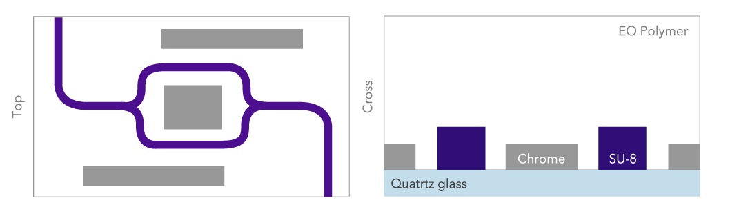
It comprises an SU-8 waveguide core, electrodes in the plane with the waveguide core and an EO polymer coating. The waveguide device is then tested using custom developed equipment. An optical image of our SU-8 waveguide splitter can be seen below. The device operation with excited first mode in the MZI is shown as well.


