
We use cookies to provide great user experience. By continuing on this site you accept use of the cookies.
We use cookies to provide great user experience. By continuing on this site you accept use of the cookies.


Investigation of organic materials and prototyping of organic light emitting diodes (OLED) for innovative screens and lighting applications
Materize is a highly competent player in organic materials. This includes both aspects: original material research; as well as technical possibilities to fabricate experimental devices for various organic materials’ applications. Also, broad options of characterisation of materials and devices are available.
Organic materials are used in many innovative applications as organic light emitting diodes (OLED) for screens and lighting devices, transparent and flexible organic photovoltaics (OPV), optical modulators etc. Our modern infrastructure allows for working with any application of organic materials.
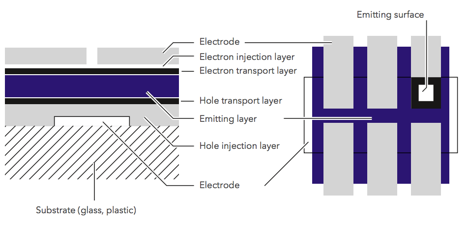
In our OLED example you will see many of the possibilities we can offer. We will make and characterise an organic light emitting diode after the particular design seen below. The thickness of each layer varies from 0.5 nm to 200 nm.
The fabrication of the OLED device takes place in our cleanrooms with an ISO classification of 7-8. We have the only classified laboratory cleanrooms in Latvia; suitable for setting up material acquisition technologies and research into materials science and nanomaterials.
The substrates have been cleaned up to standard, including an ultrasonic bath and ozoniser. For our OLEDs, we use transparent ITO substrates to form the bottom electrode, but other different materials can be used, and any shape of bottom electrode can be created.
To fabricate your own device, we can offer you commercially available materials to work with, or you are welcome to bring your own materials. We have also established broad collaboration with chemists from many countries, enabling us to develop new original organic materials. In the case pictured here we used an original light emitting-material for the OLED, synthesised by our partners – chemists from Riga Technical University.
We use several methods to produce all the required layers for our device. One of the methods is wet chemical coating. For materials that can be damaged by oxygen, a wet chemical coating can be applied in an inert atmosphere (Ar), as was the case for our OLEDs. For that reason we have a spin-coater placed in the glovebox and, also, all solutions are prepared in the glovebox. If we need to transport the device to other systems, we use a specially designed box, thereby ensuring that devices are kept in an Ar atmosphere.
Another method for fabrication of thin layers is thermal evaporation in vacuum. We have decades of experience in thin-film preparation by material thermal evaporation in vacuum. The thermal evaporation in vacuum of organic and metallic materials can be combined with magnetron sputtering and plasma cleaning methods in the SAF 25/50 vacuum coating cluster system located in the clean-room facilities, where devices are easily transported in-between various process chambers by an automatic manipulator. All processes are managed through control software.
To fabricate an organic layer and upper electrode for our OLEDs, in this case, we use the SAF 25/50 vacuum coating cluster. We place the device in the system through a glovebox to ensure an inert atmosphere.
First we add a sublime organic layer, and then the upper metallic electrode. In our case, it is aluminium, but we can make thin films from many different metals. During the sublimation process we can control thickness, sublimation rate and substrate temperature. In our cluster system, we can reach a vacuum of 1×10⁻⁶mbar.
Our OLED device is ready after encapsulating in a protective layer, carried out in a glovebox with inert Ar atmosphere.
For OLED devices, we can measure electroluminescence and photoluminescence; we can also determine the colour of electroluminescence in CIE coordinates and current-voltage-brightness characteristics, giving us information about the efficiency of our device (current and power efficiency). Knowing all these characteristics, we can tell whether the OLED we have made is better than those on the market.
Prior to fabrication of our OLEDs, we carry out: ionisation energy measurements (photoelectron spectroscopy method, determination of the energy structure of materials forming OLED), electron affinity energy determination (spectral dependence of intrinsic photoconductivity, determination of the energy structure of materials forming OLED), luminescence spectra measurements (determination of emission spectra of compound), photoluminescence quantum yield determination (determination of the highest possible efficiency of OLED), and charge carrier mobility determination (time of flight technique).
We also do analysis of morphology of all deposited layers using a high-resolution optical microscope (on the left) and scanning electron microscope (on the right).


