We use cookies to provide great user experience. By continuing on this site you accept use of the cookies.
We use cookies to provide great user experience. By continuing on this site you accept use of the cookies.


Cleanroom based platform for development and testing of new ideas in micro and nano technologies
The Prototyping Laboratory is a facility in the cleanroom area of 680 m². Process and measurement tools provide a broad platform for the development and testing of new ideas in micro and nano technologies, based on CMOS-line technologies. ISO class 7-8.
Spin-coater Laurell (2 installed)
Thermal evaporation Edwars auto 306
Sputter cluster SAF25/50
Magnetron sputtering cluster tool for process research and thin-film deposition
Atomic layer deposition
Plasma enhanced chemical vapor deposition (available 2020 Q1)
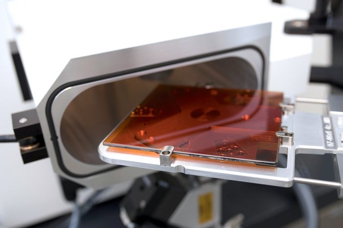
Thickness measurements
Determines thin-film thickness and optical constants. Also composition, crystallinity, roughness, doping concentration, and other material properties associated with a change in optical response can be detected.
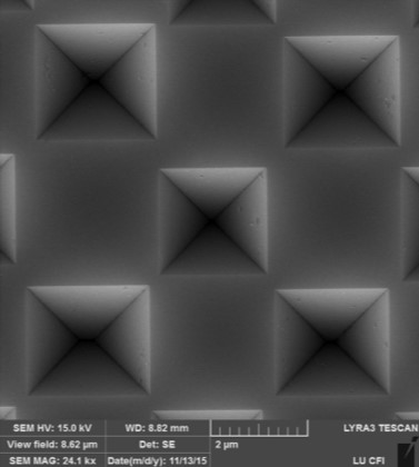
Electron microscopy
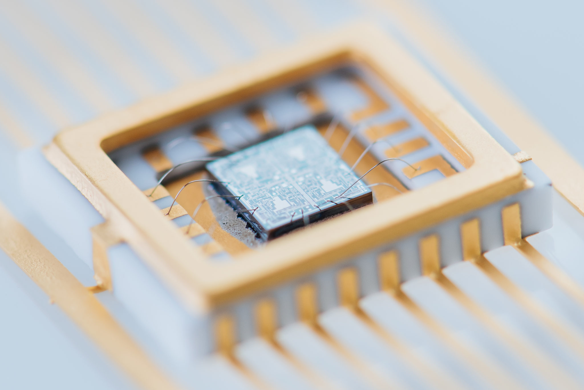
Wire bonder
Making interconnections (ATJ) between an integrated circuit (IC) or another semiconductor device and its packaging during its semiconductor device fabrication.
Probe station
Physically acquires signals from the internal nodes of a semiconductor device.
Dicing saw
High-speed spindle fitted with an extremely thin diamond blade to dice, cut, or groove semiconductor wafers, silicon, glass, ceramic, crystal, and many other types of material.