
We use cookies to provide great user experience. By continuing on this site you accept use of the cookies.
We use cookies to provide great user experience. By continuing on this site you accept use of the cookies.


We can start with creating theoretical models of materials, continuing on to creation of the material, its testing, and developing the material with the desired properties. For the next steps we offer the creation of a proof-of-concept device in a laboratory environment followed by a prototype targeted to a real-life environment.
With our industrial partners, for example, the well-known LCD developer EuroLCDs, we can go through the industrialisation process, starting with small-scale production of the first components based on new functional materials. These services are available for SMEs, big industrial customers, and academia.
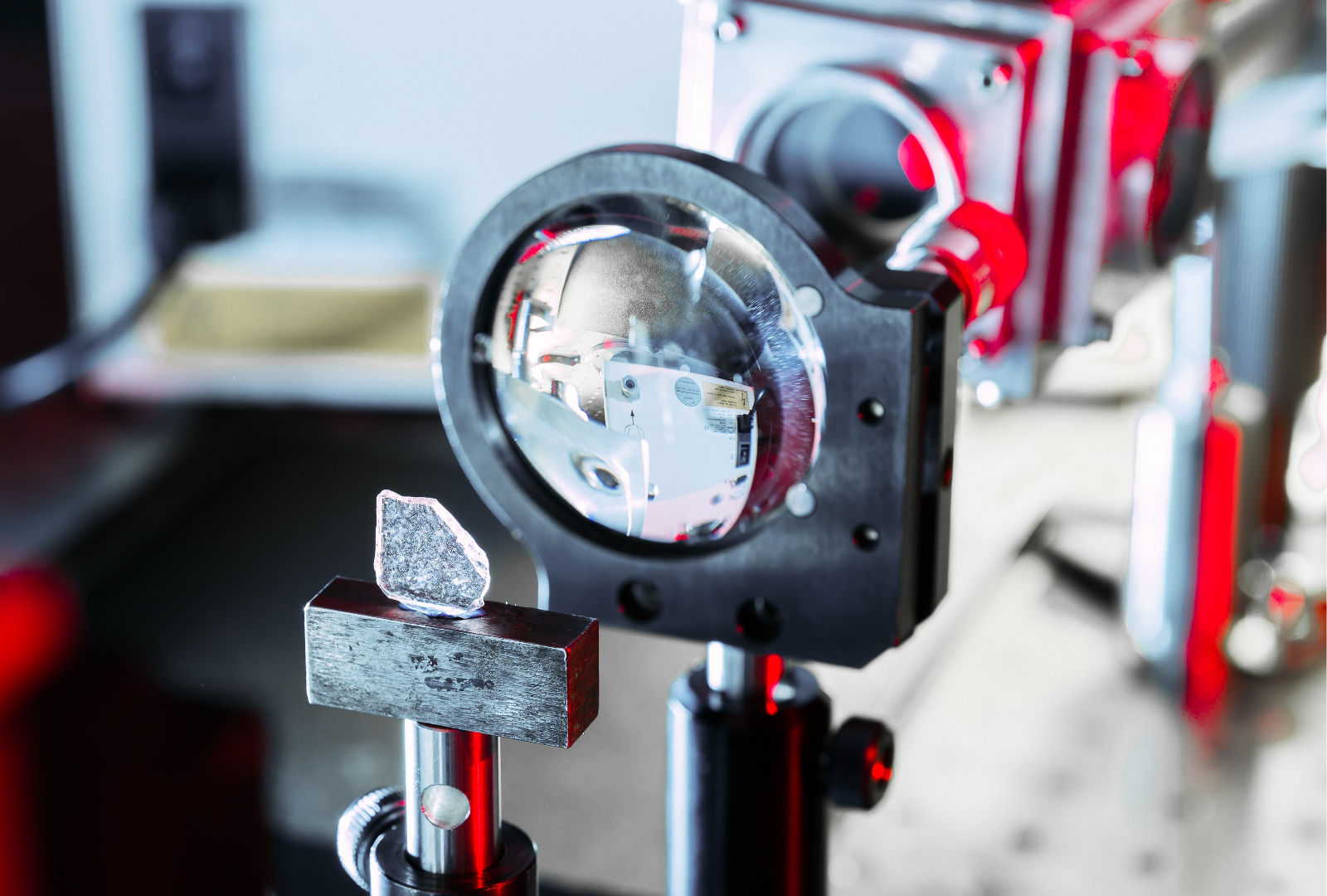
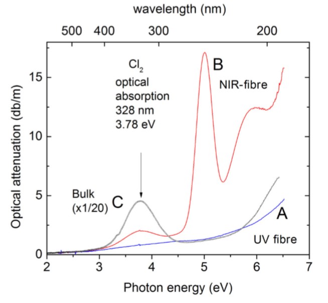
One of our strong competencies is expertise in SiO2. Using various spectroscopic methods, we can study SiO2 in its multiple crystalline, glassy and amorphous forms. We can also develop various amorphous oxide materials related to SiO2, such as germanosilicate glasses and multi-component silicate glasses. These materials can be studied in bulk (monocrystals, polycrystals, glasses), thin film, fibre and nanoparticle forms.
Together with our partners, well-known optical fibre companies Ceramoptec and Light Guide Optics, we can develop fibre optic solutions for your needs.
In addition to many other materials, we work a great deal with organic semiconductor materials. Together with our partner, start-up company Evoled, we are developing innovative materials for OLEDs.
We can offer a full cycle, from material selection and research right up to prototyping of OLEDs in our cleanrooms.
To characterise an OLED device, we can measure electroluminescence and photoluminescence. We can also determine the colour of electroluminescence in CIE coordinates and current-voltage-brightness characteristics that give us information about the efficiency of the device (current and power efficiency).
